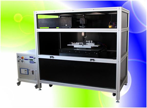
This system is multifunctional laser cutting system for micromachining of many different materials like: metal foils from copper, bronze, brass, aluminium, stainless steel and also materials like: ceramic, diamond and graphite. But according to its application, this system was designed especially for producing metal stencils in stainless steel foils used for applying solder paste during PCB manufacturing process in SMT technology. Thicknesses of these foils are varied between 80-200 um), which depends on pads dimensions (the smaller pad the thicker metal foil is used). This system is based on new generation DPSS Nd:YAG laser (l=532 nm) which generates laser beam with average output power of 12 W. This allow to cut metal foils with thicknesses amount to even 0,5 mm.

A real view of the laser micromachinig system ULMM-1
more »
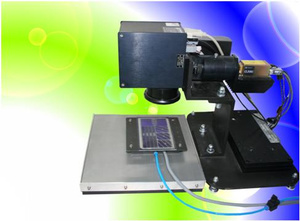
Laser Direct Imaging (LDI) technology is used for imaging electric circuits directly on PCB without the use of a phototool or mask. We presents our laboratory system for Laser Direct Imaging designed for tracks and spaces on PCB with minimum track/space widths distance of 50/50 µm. In our research we used photoresist with 50 µm resolution, but in case of using laser photoresists with better resolution (e.g. 25 µm) it is possible to image tracks in super-fine-line technology (25/25 µm).

A view of a real laboratory system for LDI
more »
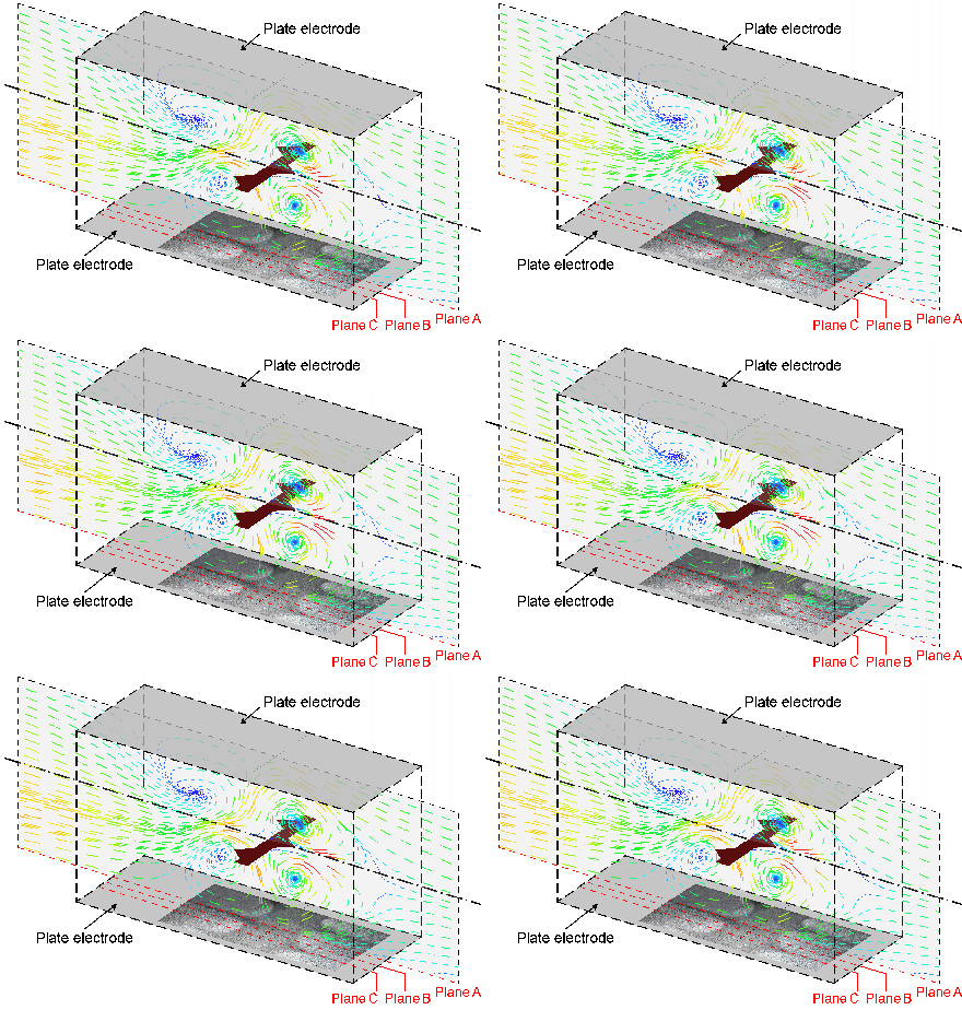
The PIV method based on the scattering of laser light on the particles following the flow has been introduced to measuring the flow velocity fields in large cross-sections of the flow. This method gives the unique possibility to measure the velocity field in the flow with a high electrical field, especially in turbulent flows and vortical structures.

more »