Laser direct imaging
Laser Direct Imaging (LDI) technology is used for imaging electric circuits directly on PCB without the use of a phototool or mask. We presents our laboratory system for Laser Direct Imaging designed for tracks and spaces on PCB with minimum track/space widths distance of 50/50 µm. In our research we used photoresist with 50 µm resolution, but in case of using laser photoresists with better resolution (e.g. 25 µm) it is possible to image tracks in super-fine-line technology (25/25 µm). Our laboratory system for LDI consist of diode UV laser (λ=355 nm, P=9 mW), optical scanner head, telescope and XY planar table, which extends scanner head working area into 15 x 25 cm usable area. A sophisticated computer software was developed to control this system.
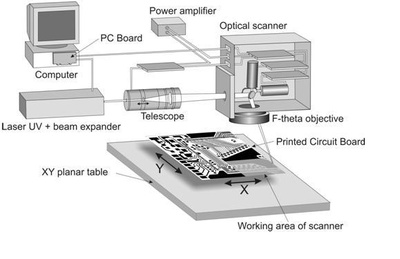
Fig. 1. Scheme of LDI system connections
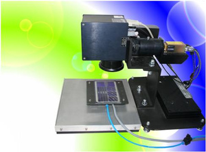
Our system consists of four major components: the UV diode laser (λ=375 nm), the telescope, the optical XY scanner and the XY planar table (Fig. 1). The UV diode laser generates CW laser beam at average output power of 9 mW. The optical scanner has built-in two high speed galvo-drivers with mirrors, which allows to displace focused laser beam with maximum velocity of 1 m/s. The scanner head is connected to a computer through a PC card. To focus the laser beam, the F-Theta objective (f = 100 mm) is used. Laser beam has 0.9:1.1 ellipticity, spot size of 1.1 mm, divergence (half angle) of 0.5 mrad and beam shape (far field) circular. The minimal spot size observed after the optical path length (after telescope and F-Theta objective of optical scanner) was 32 µm (using laser beam analyzer Spiricon LBA-300). The working area of the scanner head is 6 cm x 6 cm. A computer controlled telescope can dynamically change the laser beam divergence, which allows to change slightly a laser spot size over the working area of the scanner. XY planar table is used to expand working area of the whole system. It make possible to produce patterns over PCB surface in maximum area of 15 x 25 cm. At the moment, system for LDI allows to work in two dimensional area only. In the future, there will be movable Z table over XY planar table, which expand all system capabilities. It will be possible to manufacture three dimensional shapes or elements made from special dry photoresists, which cure upon influence of UV laser beam radiation. 3D figures will be imaged layer by layer with micrometer resolution. This technique is suitable for small elements prototyping and can be used e.g. in medicine. On Fig. 2 a real view of our laboratory system for LDI is presented.
Fig. 2. A view of a real laboratory system for LDI
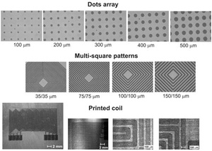
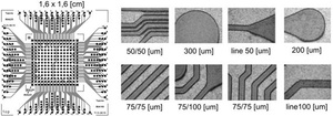
During experiments of laser direct imaging on conventional photoresist KOLON, which photosensivity was 35- 50 mJ/cm2, we put a major impact on imaging tracks 50/50 µm. Tests were carried out on conventional photoresist to prove, that widely used conventional photoresist is suitable for LDI technology. The use of conventional phoresist is important for PCB manufactures, since the new LDI technology should be compatible to PCB’s production process. During tests the imaging speed, frequency, amplitude of circular movement, overlapping of the adherent lines and also average power of a laser beam were changed and optimal parameters for each operating modes of LDI system were found. On Fig. 3 dots array, multi-square patterns and printed coil are presented. The best result of high density interconnects was achieved with multi-square pattern and it was 35/35 µm (track width/space width).
Fig. 3. Examples of different patterns on PCB, which show capabilities of control program for LDI system
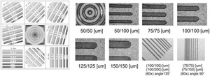
Fig. 4. Preview of test pattern consisted of lines with different widths and angles and circle patterns
Fig. 5. Preview of BGA (Ball Grid Array) pattern and magnified photoresist tracks
